SCIENTIFIC & TECHNICAL SERVICES

Electron Microscopy Service

An advanced electron microscopy service in Barcelona providing SEM and TEM characterization for materials science research, nanostructures, surfaces and devices.

SEM and TEM characterization for advanced materials

The Electron Microscopy Service was created in 2008 and is mainly dedicated to ICMAB research groups, while also being accessible to external users.

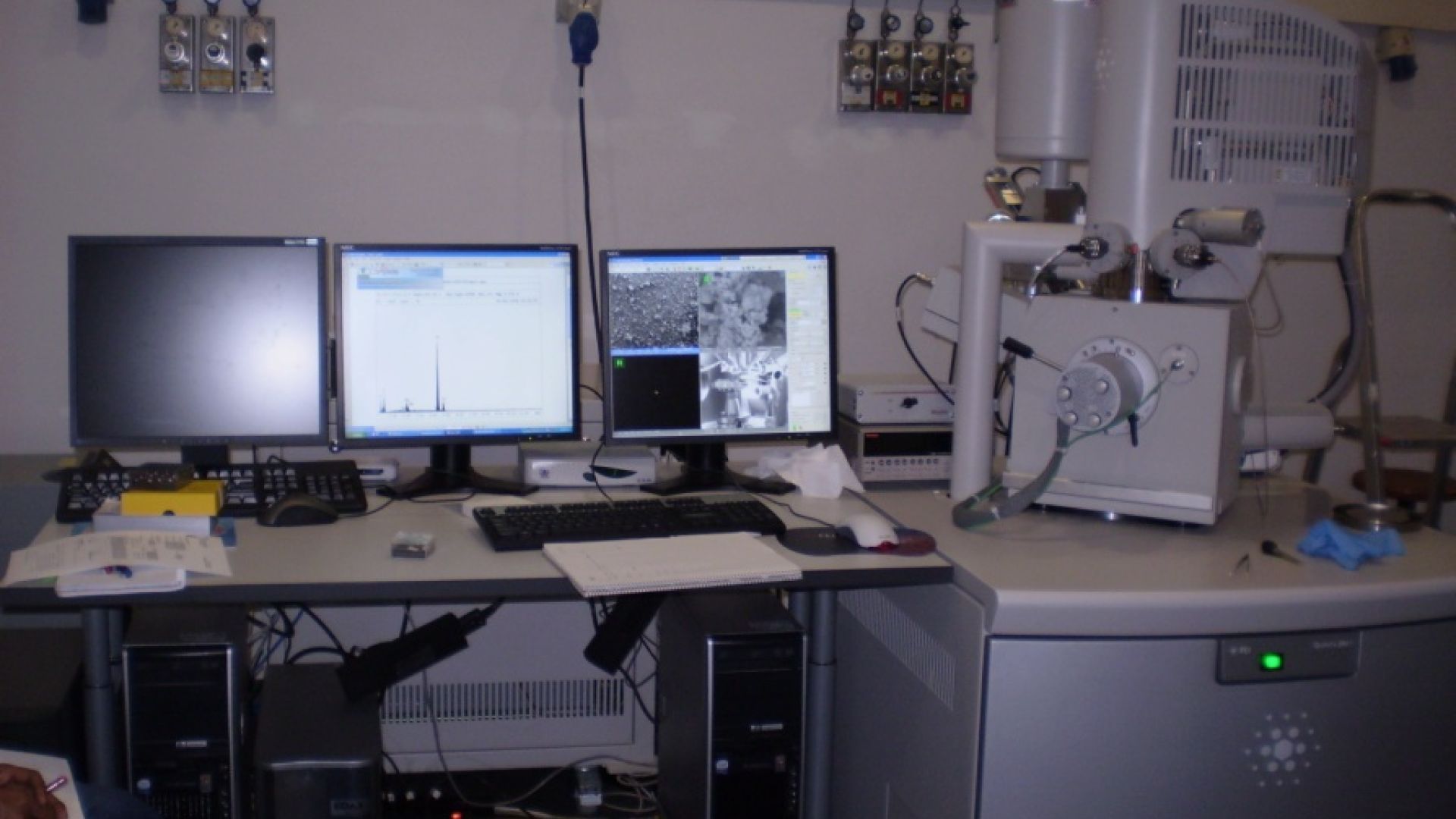
The service provides SEM and TEM materials characterization through a Scanning Electron Microscope QUANTA FEI 200 FEG-ESEM and a Transmission Electron Microscope JEOL 1210.

Its mission is to support high-profile nanostructural characterization in-house, reducing technical limitations and providing advanced imaging, microanalysis and electron diffraction capabilities for materials science research.

Electron microscopy capabilities

A scientific platform for morphological, structural and chemical characterization of materials at the micro- and nanoscale.

SEM imaging

High-resolution scanning electron microscopy for surfaces, nanostructures and materials inspection.

TEM analysis

Transmission electron microscopy for morphology, microstructure and diffraction studies.

EDX microanalysis

Chemical analysis, elemental mapping and line scans for complex materials.

Training & support

Technical support, electronic management and user training for efficient self-service operation.

Equipment

The service combines SEM and TEM instrumentation to provide complementary information on morphology, composition, microstructure and diffraction.

Scanning Electron Microscope SEM

Scanning Electron Microscope (SEM) QUANTA FEI 200 FEG-ESEM

The Quanta 200 ESEM FEG from FEI is a special and advanced type of high performance scanning electron microscope (SEM). The FEI Quanta 200 FEG is a state of the art field emission microscope that allows nanometer level inspection of materials.

It is equipped with a field emission gun (FEG) for optimal spatial resolution. The instrument can be used in high vacuum mode (HV), low-vacuum mode (LV) (water vapour injection), and environmental SEM mode (ESEM). This makes it possible to study samples in pressures up to 5 Torr. It is engineered to provide maximum data with non-destructive analytical techniques- imaging and microanalysis – from all types of specimens, with or without preparation. The microscope is equipped with an Energy Dispersive X-ray (EDX) system for chemical analysis. Qualitative and quantitative analysis, elemental mapping and linescans can be performed. Lithography and nano-lithography can be performed by a RAITH e-beam.

The scanning electron microscopy service, equipped with a QUANTA FEI 200 FEG-ESEM offers a powerful imaging tool for both, routine and advanced inspection of materials. The service is intended to offer high resolution facilities (1.2 nm @30kV) with a field emission gun, specially suited for the morphological characterization of nanocrystals, nanostructured materials and surfaces. Image contrast proportional to the atomic number is also available with high lateral resolution (2.5 nm @30kV) using an electron backscattered detector. The instrument can be used in high vacuum mode, low-vacuum mode (the chamber pressure is monitored by water vapour injection), and environmental SEM mode (ESEM). This makes it possible to study samples in pressures up to 5 Torr. The resolution is kept high at all conditions: 1.2 nm and 1.5 nm at 30kV in the high and low vacuum modes, respectively. The capability to vary the chamber pressure is specially suited for the observation of uncoated non-conducting materials. The microscope also features an EDS detector designed for light elements starting from Be, with an energy resolution of 132 eV. This tool enables the chemical analysis with a high lateral resolution (point analyses and elemental mapping), as required for the characterization of complex multicomponent nanostructured materials. The service includes electron beam lithography, used in many research activities at ICMAB like development of organic devices, the fabrication of substrate templates designed for defect engineering in thin epitaxial superconducting films, investigation of surface self-organization phenomena, and the fabrication of magnetoelectronic devices. Lithography and nano-lithography can be performed by a RAITH e-beam.
An environmental SEM, enabling characterization of non-conducting without a conductive, and is equipped with EDS (light element) and electrón-beam.
 
image003
SEM pictures of different materials obtained by the Scanning Electron Microscope QUANTA FEI 200 FEG-ESEM

Transmission Electron Microscope TEM
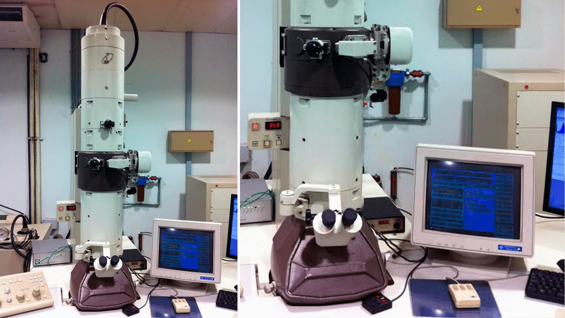
Transmission electron microscope (TEM) 120 KV JEOL 1210

The 120 KV JEOL 1210 TEM features a high angular range (Tilt X= ± 60o, Tilt Y= ± 30o) providing a unique facility in the area of Barcelona for exploring large volumes of the reciprocal lattice by electron diffraction. It has technical support by a high profile (Dr) staff member. With a resolution below 3.2 Å this equipment is useful for low resolution structure imaging and characterization of nanoparticulate systems.

When operating in image mode TEM provides information about the size, morphology and microstructure of the samples.In diffraction mode, it allows the determination of the cell parameters, space group and superstructures, incommensurate modulations, etc. The transmission electron microscope service is equipped with:

  • Holder: Analytical specimen holder, doble tilt ( Tilt X=± 60o, Tilt Y=± 30o ) GATAN 646.
  • Camera: ORIUS 831 SC 600, GATAN.

Imagen1 1

TEM pictures of different materials obtained by the Transmission Electron Microscope  JEM-1210 (JEOL), operating at 120 KV

Booking calendar

Check the SEM booking calendar before requesting a session. Reservations are managed by the service team and should be requested in advance according to the rules of use.

Request SEM or TEM service

The Electron Microscopy Service provides different access procedures for SEM and TEM sessions. Review the booking rules, required forms and results folders before using the service.

Request SEM Service

RULES OF USE

 To obtain for a session you need to do the following:

  1. Check to see availability for your group on the booking calendar
  2. Ask by This email address is being protected from spambots. You need JavaScript enabled to view it. with proposed times and your department’s name. This needs to be done 24H prior to the session’s start. Note that this is a first-come first-serve system for allocating time within your group’s department. If there are time slots which are not used, then other people from outside that department may use it.
  3. Fill out the appropriate form and have it signed. This form can be found in the folder marked “GRUPO” and then “SEMQUANTAFEI” or in this web. 

___________________________________________________________________________________________________

Timetable of Reserves


Dilluns

Dimarts

Dimecres

Dijous

Divendres

9:00h-11:00h

Servei de Microscòpia

SOLID STATE CHEMISTRY

11:00h-13.00h

CMEOS
CRYSTALLOGRAPHY
NN

MULFOX
ACNM

LMI
FUNNANOSURF

SUMAN

13:00-15:00h

NANOMOL

SURFACES
NANOPTO
LASER

SUMAN

MULFOX
ACNM

CMEOS
CRYSTALLOGRAPHY
NN


RESULTS

Grupo\semquantafei

Request TEM Service

Electron Microscopy Service team

Technical staff, scientists in charge and user committee members supporting SEM and TEM access, training and characterization workflows.

Technicians


Scientists in charge


User's Committee

Electron microscopy image gallery

Examples of SEM and TEM images obtained through the Electron Microscopy Service for different materials and nanostructures.

Contact Electron Microscopy Service

ICMAB
Campus UAB
In front of Firehouse
08193 Bellaterra
Barcelona, Spain
E-mail

Phone