Scanning Probe Microscopy
A scientific service for nanoscale surface characterization using atomic force microscopy, scanning tunneling microscopy and advanced SPM modes for materials science research.
Nanoscale imaging and local surface characterization
The Scanning Probe Microscopy Laboratory offers SPM-related experiments to the ICMAB community and to external scientific users.
The service is open to researchers from research centres, universities, technological centres, spin-offs and industry, including international users and researchers working within the NFFA Europe project initiative.
The laboratory provides access to advanced SPM instrumentation for nanoscale topography, electrical, magnetic and functional characterization of materials and devices.
Main service capabilities
Advanced scanning probe microscopy capabilities for nanoscale surface imaging, local electrical characterization, magnetic contrast and functional materials analysis.
AFM imaging
Functional SPM
STM measurements
External access
Scanning Probe Microscopy equipment
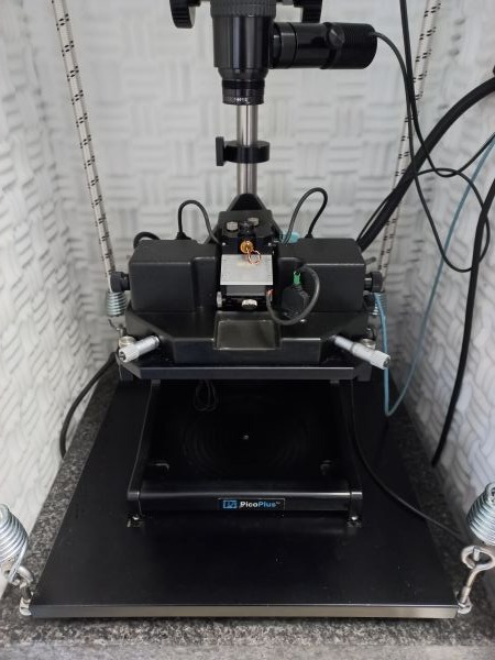
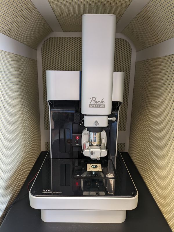
The SPM Lab combines Park System NX10 and Keysight 5500 AFM instrumentation for advanced nanoscale measurements and flexible lock-in based experiments.
Park System NX10
Scanner
- 100 μm × 100 μm range in XY
- 15 μm range in Z
Stage
- XY stage travel range of 20 mm × 20 mm
Optical microscope
- Tip possitioning by optical microscopy
- Field of view: 480 μm × 360 μm
- 10 × objective lens
Sample mounting
- Sample size: Open space up to 100 mm x 100 mm, thickness up to 20 mm
4 channels of flexible digital lock-in amplifier
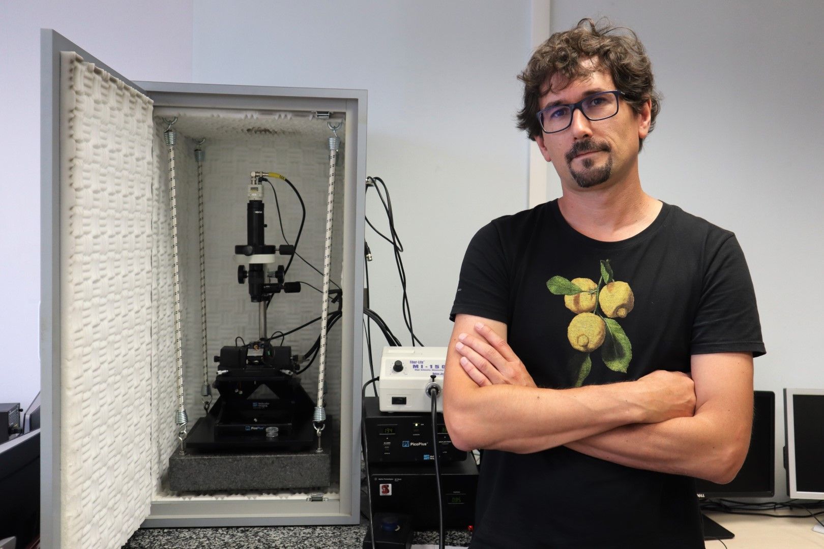
Keysight 5500 AFM
- Piezoresponse Force Microscopy
- Bimodal Atomic Force Microscopy
- Dynamic Topography.
It also has a Closed Loop capability that significantly improves the positioning in X and Y.
Sample size is limited to 3 x 3 cm in the X and Y directions and 1 cm in the Z direction.
A Q-Control is also available to enhance images in liquid.
SPM modes and measurement capabilities
The laboratory supports a broad portfolio of AFM and STM measurement modes for structural, electrical, magnetic and functional characterization.
Atomic Force Microscopy modes
- Contact mode
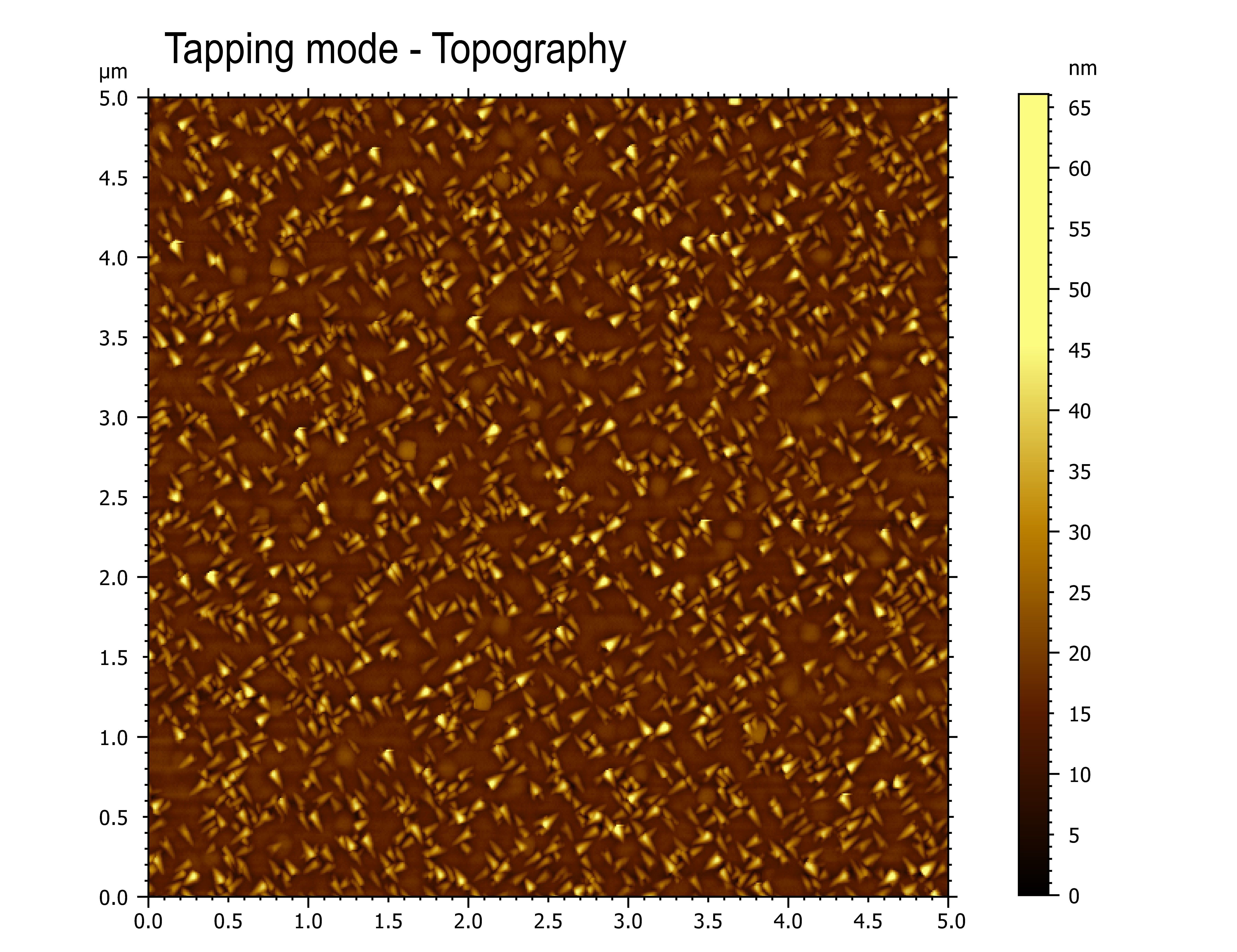
- Tapping mode
- Non-contact mode
- Friction Force Microscopy (FFM)
- Electrostatic Force Microscopy (EFM)
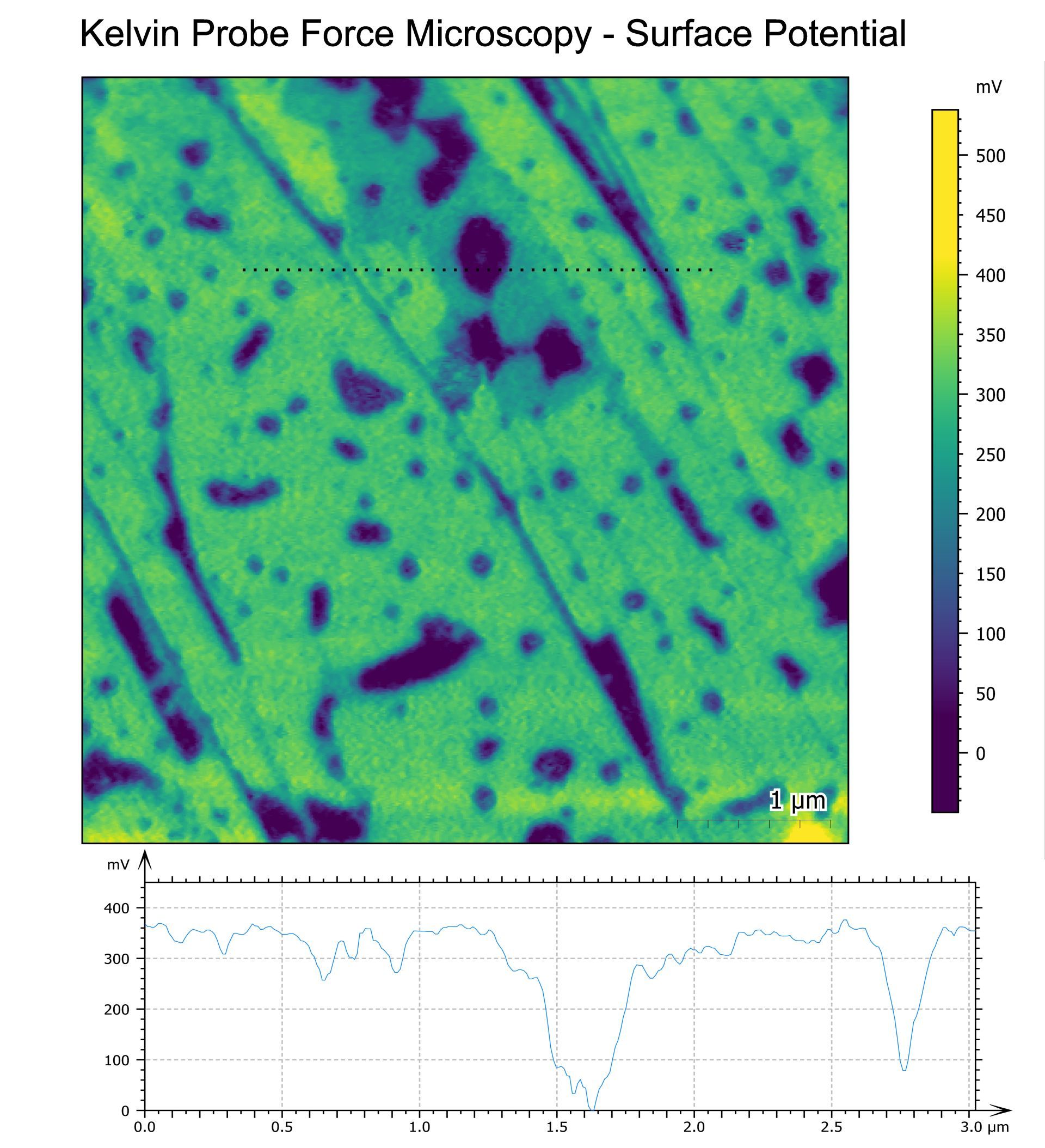
- Kelvin Probe Microscopy (KPFM)
- Piezoresponse Force Microscopy (PFM)
- PinPoint AFM
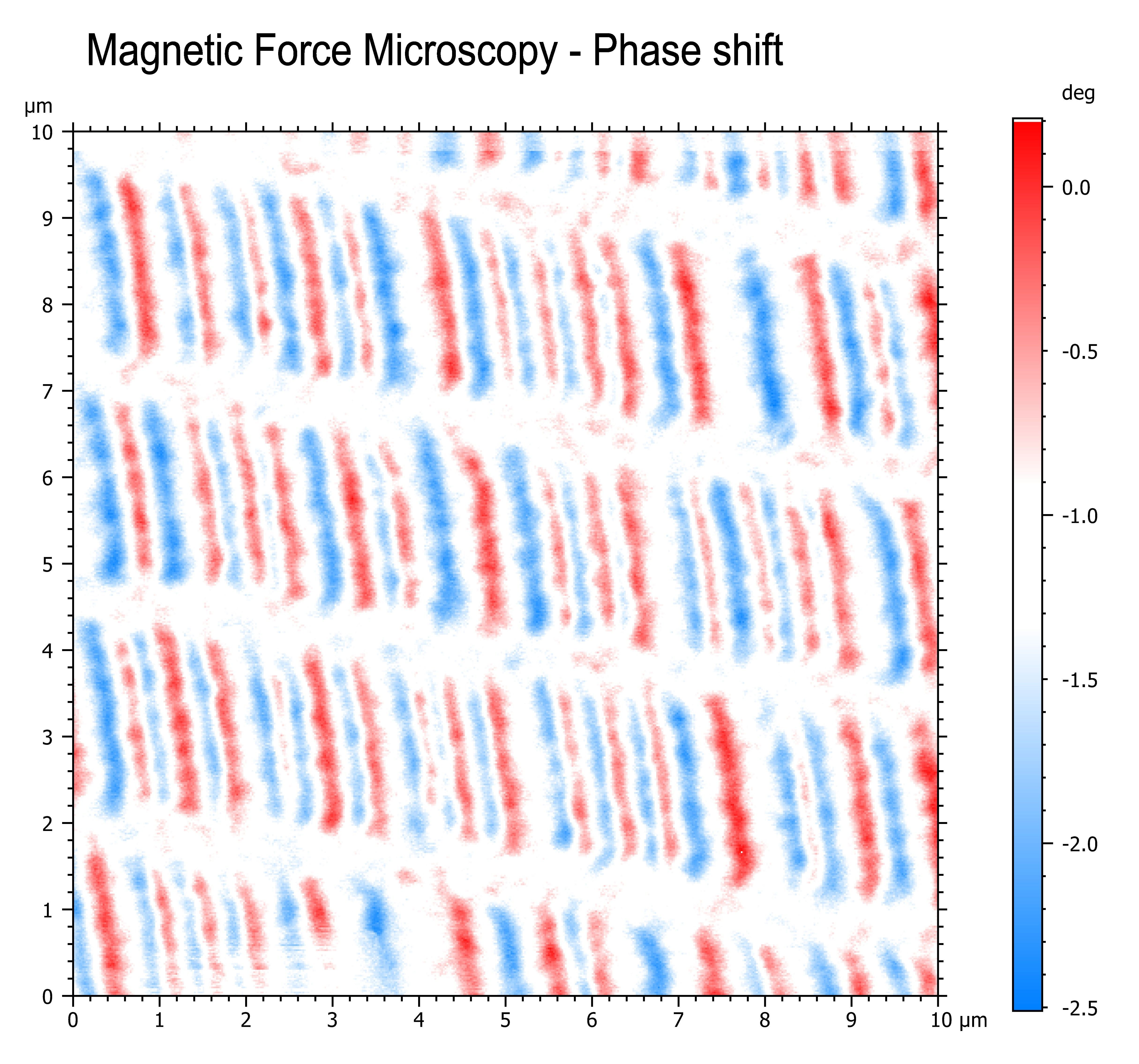
- Magnetic Force Microscopy (MFM)
Scanning Tunneling Microscopy modes
- Constant current mode
- RT and controlled atmosphere (N2)
How to request a service
Submit the service request form and the SPM team will contact you to define the measurement needs, sample requirements and access conditions.
You can also contact the laboratory by email for specific questions or special requests.
1
Submit the service request form.
2
The SPM team reviews your needs.
3
Define sample, mode and measurement strategy.
4
Carry out SPM experiments.
5
Receive images, data and technical feedback.
Open for NFFA Europe users
Open for NFFA Project
Scanning Probe Microscopy team
Technical staff, scientist in charge and user committee members supporting access to SPM instrumentation and nanoscale characterization workflows.
Technicians
Scientist in charge
User's Committee
SPM image gallery
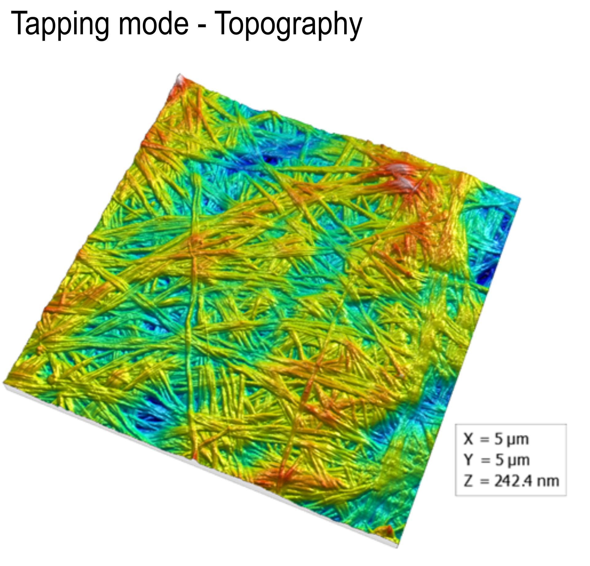
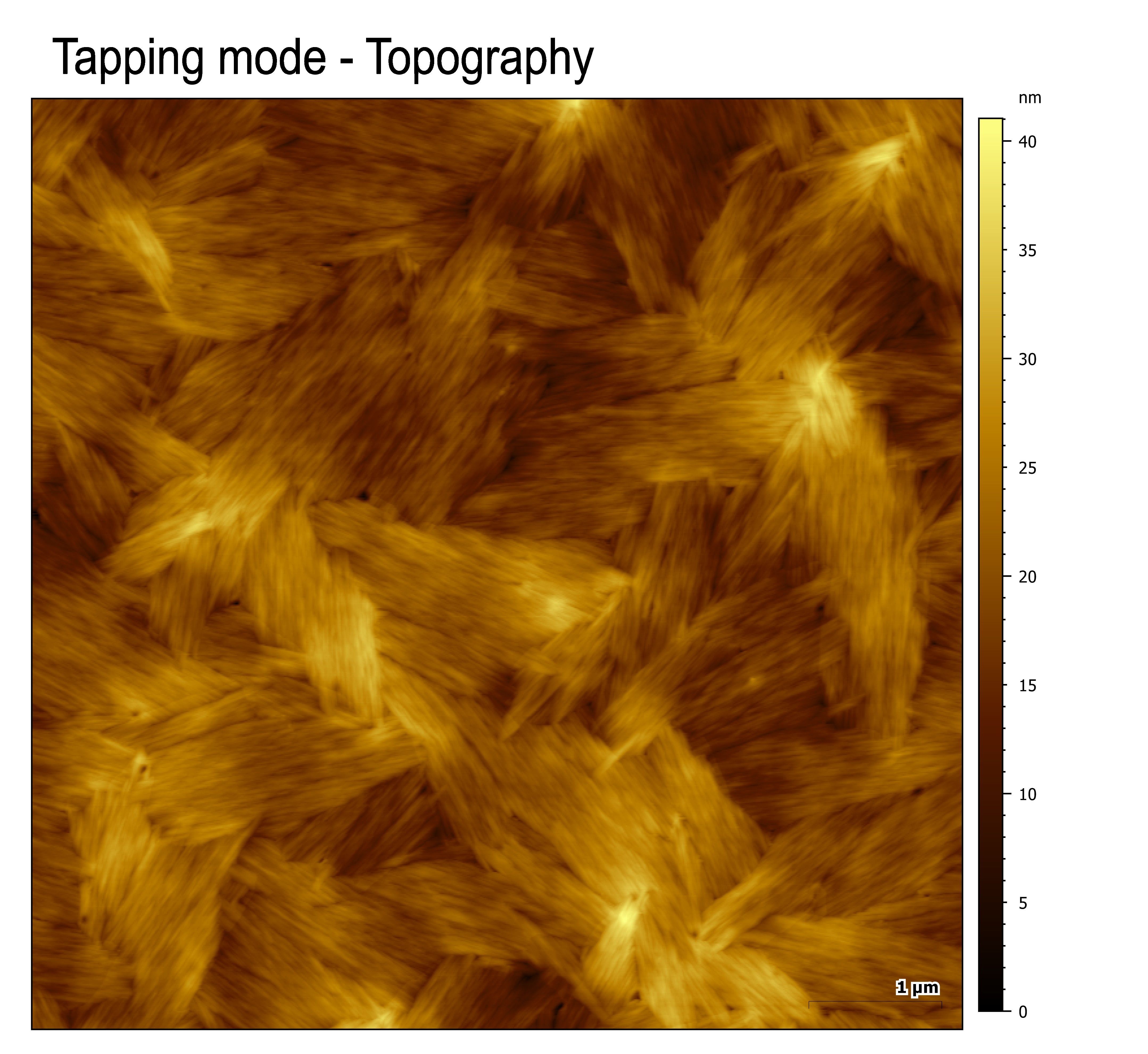
Examples of nanoscale imaging and functional characterization obtained through SPM techniques.
Contact Scanning Probe Microscopy
ICMAB
Campus UAB
08193 Bellaterra
Barcelona, Spain

Phone
ICMAB - Scanning Probe Microscopy
OpenStreetMap service required
to load this map.
OpenStreetMap service required
to load this map.